Focused Ion Beam
What Is It?
The Focused Ion Beam (FIB) technique is analogous to Scanning Electron Microscopy (SEM) in that it scans a focused probe beam, in this case ions rather than electrons, across the surface of interest.
Why Should I Use It?
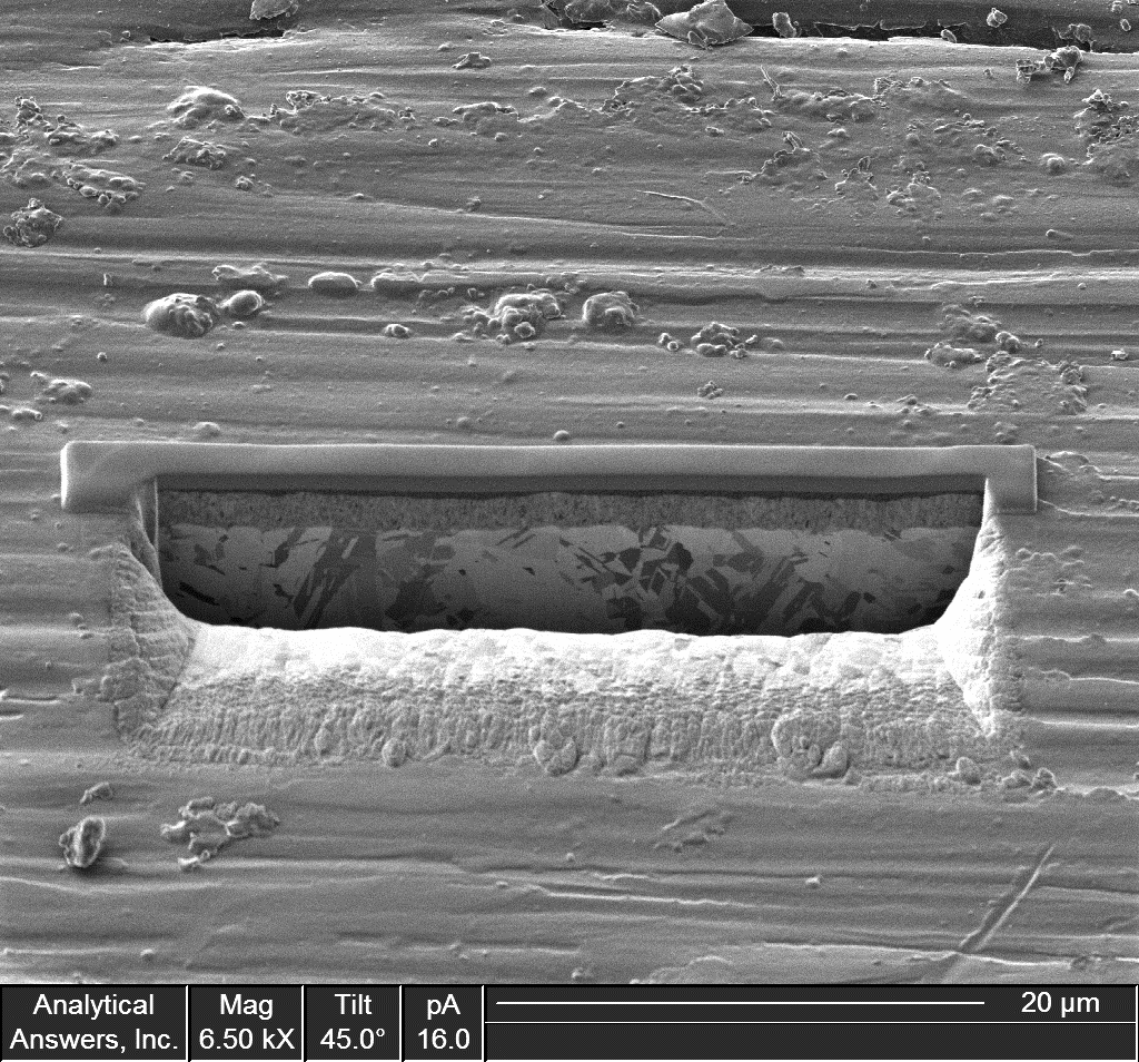
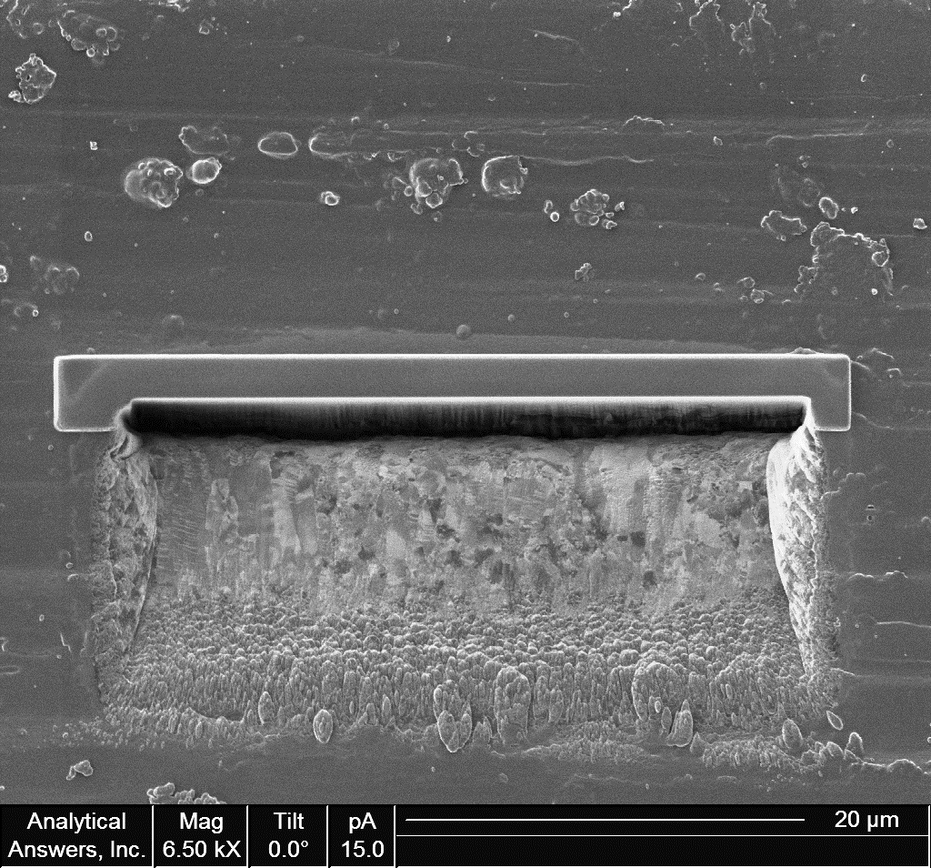
This beam can be used to generate high-resolution images of the sample or to mill into the sample to expose the internal structure.
What Do I Get Out of It?
This combination of high-resolution imaging to locate features of interest followed by precise site-specific milling provides an invaluable tool for sample preparation and analysis, providing rapid cross-sectional analysis of features that would be difficult or impossible to otherwise prepare. Because of this, the FIB instrument is often used as a sample preparation tool for more complete characterization using Electron Microscopy.
Applications Include:
- Materials Evaluation
- Process Development
- Protective coatings
- Inclusions
- Grain size distributions
- Layered structures
- X-sections of hard to polish materials
- Micromachining
- Failure Analysis
- Precise site-specific cross-sections
- Sub-surface contamination/defects
- Delamination
- ESD damage
- Quality Control
- Layer thicknesses
- Etch profiles
- Step coverage and conformality