Capabilities
The core strength of Analytical Answers is our flexibility: our willingness and ability to work along side our clients, wherever you are, whatever your need. We offer Anywhere™ Services to help you get the answers you need, quickly.

We use a wide variety of analytical tools, selected to best meet your specific needs.
Click here for an overview of applications and the tools that serve them.
Descriptions
Below we provide you with an introduction to some of our most utilized instruments and techniques. Don’t see what you need here? We offer many more services. Contact us using our form and we will reply with a custom solution.
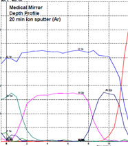
Scanning Auger Microscopy (also known as Auger Electron Spectroscopy) analyzes conductive samples at a depth of 2-3 nm. And with our high-accuracy instrumentation (field emission source) we have the ability to sample with a lateral resolution of better than 30nm. This allows for the inspection of films with the thickness of only a few monolayers from top down, or layers a few tens of nanometers thick when examined in cross section. Auger analysis can detect all elements except hydrogen and helium, at concentrations as low as 0.1 atomic percent (depending on element and matrix). An in situ ion beam can be used to remove material from the sample to allow analysis of buried layers. These so-called Depth Profiles produce plots of composition versus depth and can extend up to several microns below the surface. While Auger analysis performs best on semiconductors or conductive samples, less-insulating materials can sometimes be analyzed.
Understand it better
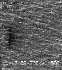
Variable Pressure Scanning Electron Microscopy is a technique used to produce high resolution images with a high depth of field. VPSEM differs from traditional SEM in that the instrument chamber is operated at higher pressures (~10 Pa to 3,000 Pa) which allows for imaging and analysis of insulating samples without the need to apply a conductive coating.
This is convenient for when it is undesirable to coat a sample or the sample is too large for the coating systems.
With VPSEM, we can examine a sample’s topography, structure, and its elemental composition under magnifications of up to ~10X to ~20,000X. Multiple electron and x-ray detectors can be employed to expose even more information about the characteristics of a sample.
Understand it better
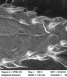
The Focused Ion Beam (FIB) technique is analogous to Scanning Electron Microscopy (SEM) in that it scans a focused probe beam, in this case ions rather than electrons, across the surface of interest. This beam can be used to generate high-resolution images of the sample or to mill into the sample to expose the internal structure. This combination of high-resolution imaging to locate features of interest followed by precise site-specific milling provides an invaluable tool for sample preparation and analysis, providing rapid cross-sectional analysis of features that would be difficult or impossible to otherwise prepare. Because of this, the FIB instrument is often used as a sample preparation tool for more complete characterization using Electron Microscopy.
Understand it better
Electron Spectroscopy for Chemical Analysis, also known as X-ray Photoelectron Spectroscopy (XPS), provides information on the atomic composition and chemical bonding of a sample on the surface (top few nanometers). ESCA can detect all elements except for hydrogen and helium, and the detection limit is about 0.1 atomic percent. We can use ESCA on both conductive and insulating samples, which mean this technique has a wide application for both organic and inorganic samples.
Understand it better
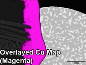
Energy Dispersive X-Ray Spectroscopy (EDS) is an analytical technique to qualitatively and quantitatively identify the elemental composition of materials analyzed in an SEM. EDS analyzes the top few microns of the sample with a spatial resolution as small as one micron. Modern, ultra-thin polymer windowed EDS can detect elements with atomic numbers greater than boron, with limits of detection as low as 0.1 weight percent (depending on material). Individual spectra can be collected from spots or areas, or EDS data can be collected as either element maps or line profiles with a spatial resolution of one micron.
Understand it better
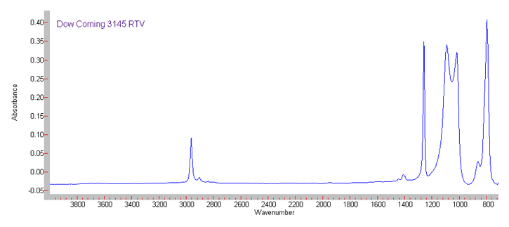
Fourier Transform Infrared Spectroscopy (FTIR) is a technique which is used to analyze the chemical composition of many organic chemicals, polymers, paints, coatings, adhesives, lubricants, semiconductor materials, coolants, gases, biological samples, inorganics and minerals. FTIR can be used to analyze a wide range of materials in bulk or thin films, liquids, solids, pastes, powders, fibers, and other forms. FTIR analysis can give not only qualitative (identification) analysis of materials, but with relevant standards, can be used for quantitative (amount) analysis.
Understand it better
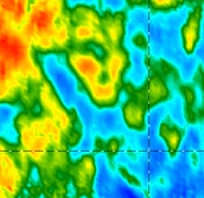
FTIR Imaging is a new technique that that provides wavelength specific high resolution infrared data that can be examined to determine chemical differences within a sample. By providing this type of data, chemical changes that could not be visualized previously, stand out in the sample, providing a much richer data set to solve problems in polymers, electronics, biological and material sciences.
Understand it better
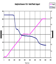
Thermal Analysis are a series of techniques that measure changes in a sample with changing temperature. The techniques measure changes in weight (TGA) or heat flow (DSC) that are characteristic of materials and formulated products.
Understand it better
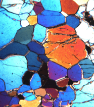
The key to any of the techniques Analytical Answers uses is the ability to “see” the sample. Visible light microscopy provides that ability.
Understand it better
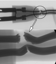
Through high-resolution X-ray microscopy, we are able to non-destructively examine the internal structure of samples in real-time, at magnifications up to 1000X. While the internal mechanisms of these samples are usually not visible under other means, XM offers us a tool to watch them in operation.
Understand it better
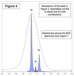
Wavelength Dispersive Spectroscopy (WDS) is a complimentary technique to Energy Dispersive Spectroscopy (EDS) for performing x-ray analysis of materials to determine their elemental composition.WDS has a much higher sensitivity to low atomic number elements, providing much better detection of elements as low as Be and B. Unlike EDS however, not all elements can be detected simultaneously.
Understand it better