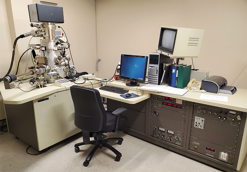
Scanning Auger Microanalysis (SAM)
Scanning Auger Microanalysis (SAM)

Scanning Auger Microanalysis (SAM) is an analysis technique that determines elemental composition and some chemistry of surfaces and interfaces. The technique has a sampling depth of 2-3 nm and is appropriate for films as thin as a few monolayers with a lateral resolution of 50 nm. It is limited to conductive samples but can also shows the spatial distribution of elements on a surface. The technique is also useful for depth profiling and will show elemental depth distributions from 1 to 2000 nm when used in conjunction with ion-milling.
Auger analysis can detect all elements except hydrogen and helium, at concentrations as low as 0.1 atomic percent (depending on element and matrix).
When information about material below the surface is of interest, an in situ ion beam can be used to remove material from the sample to allow analysis of buried layers. These so-called Depth Profiles produce plots of composition versus depth and can extend up to several microns below the surface.
While Auger analysis performs best on semiconductors or conductive samples, less-insulating materials can sometimes be analyzed.
